Buy the 27C322, 27C160, 27C800, 27C400 Programming Adapter from my store!
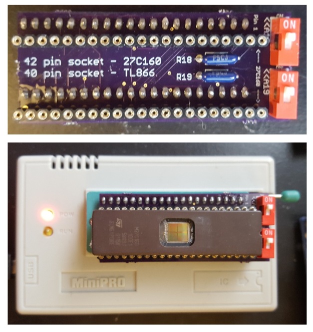
This adapter allows you to program the 27C322, 27C160, 27C800, and 27C400 chips on your TL866 programmer. The board has gone through a lot of revisions, but here’s the current model. It even has space for a ZIF socket!
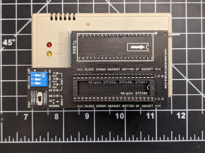
The 27C322 and 27C160 EPROMs are 42 pins wide. The TL866 and TL866II programmer only has room for 40 pins. So how are we going to deal with that? Well, the short answer is, we’re going to trick the TL866 into thinking we’re programming a different EPROM. The EPROM we’re going to tell it to program is only 4 Mbits large. Using this EPROM normally would only utilize address pins A0 through A17. The 27C322 goes up to A20, and the 160 goes up to A19. By manually controlling A18, A19, and A20 (for the 322), we can program our ROM in 4 Mbit chunks to fill up the memory space.
Assembly
View the instructions at my github page: https://github.com/MouseBiteLabs/27C322-TL866-Adapter
Splitting the ROM
If you’re following the SNES tutorial, you might already know how to do this part. If not, you can check out Step 6 of the tutorial here.
If you don’t want to use SNES ROM Utility, or are using this programmer for something other than SNES games (like, for Genesis games), you can use this utility to split the files instead. Note that it WON’T remove any header information for SNES games! But otherwise, it’s very simple to use; just load up the ROM, pick your destination folder, and type in a custom size of 512 Kbytes (which is 4 Mbits).
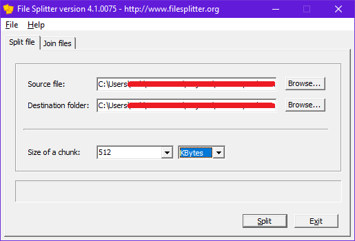
Now, you’ve got your 4 Mbit chunks to program with the TL866. These chunks will end in a .chunk001, .chunk002, etc. file extension after splitting. You can still load these files up into the programmer without any issue – no need to change the file extension back.
How to Use the Programming Adapter
Load up the 27C4096 chip on the TL866 software, and load up the first chunk from your original ROM. Change the VPP to 12.5 V, as this is dictated for programming voltage in the datasheet. Then, uncheck the “Check ID” option. Note that if you have the new TL866II and are using “Xgpro” software, you need to uncheck “Pin Detect” as well. Your window should look like this:

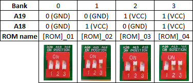
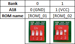
Here’s a table of how data is programmed into the EPROM. If A18, A19, or A20 is a “0”, that means tie it to GND, or if you’re using the adapter, put the switch in the “OFF” position. If it’s a “1”, that means tie it to VCC, or if you’re using the adapter, put the switch in the “ON” position. Program the 4 Mbit chunks in sequential order in the banks.
For the 27C322, use these switch positions:

For the 27C160, use these switch positions:
For the 27C800, use these switch positions:
For the 27C400, keep all switch positions OFF. Also, because the 27C400 is only 40 pins, and not 42 pins, make sure to put the EPROM with pins 1 and 42 exposed.
If you get an error while programming with the MiniPro – make sure your chips are in the correct orientation, each bank is blank, you’ve unchecked the “Check ID” box, and that you’ve selected a 27C4096 EPROM from the Select IC list! Also, make sure you’ve got the switch on the adapter board on the correct option!
How the Adapter Works
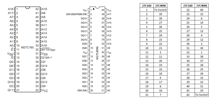
Here’s a breakdown of the pinouts on the 27C322, 27C160, and the 27C4096.
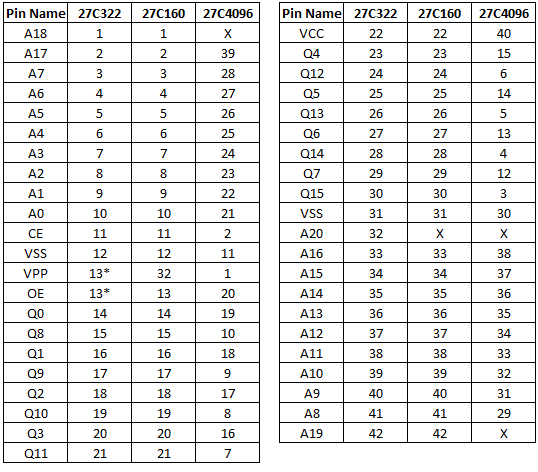
Remember, the 27C4096 is the chip we’re going to tell the TL866 we’re programming. The X’s signify an address pin that goes unused on that chip. We’ll be adding three switches to manually control these pins – A18, A19, and A20. You’ll note that the 322 and 160 share every single pin, except that 160’s don’t utilize A20, and the VPP and /OE pins are a bit different.
According to the datasheet for the 27C322, pin 13 (or /GVpp as it’s defined) combines the /OE (output enable) pin and the VPP (programming voltage) pins into one. The 4096, however, keeps these pins separate. This isn’t too much of a problem, though, if we take a look at the operating modes of the 322 we can see that we never really need the /GVpp pin to be anything but zero volts or the programming voltage.
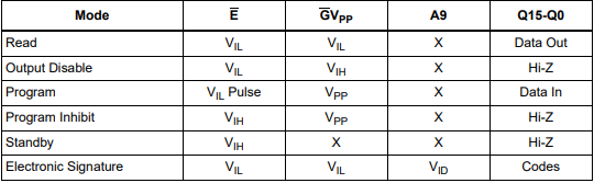
Here, VIL notates logic low, or zero volts. VIH is logic high, or anywhere between 2 and VCC + 1 volts (according to the datasheet). You’ll notice that the only mode that uses VIH is “Output Disable” which isn’t really used while programming the EPROM. So we only really need to switch pin 13 between ground and VPP (which means we can ignore pin 20 on the TL866 completely for programming the 27C322). Unfortunately, the TL866 switches VPP between the programming voltage and VCC voltage, so we need to add a bit of circuitry to change that VCC to GND.
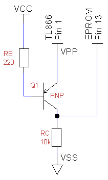
The PNP transistor above conducts when the emitter voltage is greater than the base voltage. During programming, the VPP pin from the TL866 applies the high programming voltage. When this happens, current flows through the base resistor (RB), and pulls pin 13 on the 27C322 to VPP. Then, when the VPP pin on the programmer drops to VCC voltage, the base current drops and the transistor stops conducting. This causes pin 13 to be pulled to VSS through the collector resistor (RC).
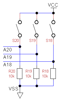
Now, taking care of the extra address pins is just using simple switches with pull-down resistors.
With this extra circuitry, we can make a standalone 27C322 adapter for the TL866. However, if you check that table again up at the top, you should’ve noticed that the 322 and 160 (and by extension, the 27C800 and 27C400) share a lot of common pins. The only real difference is which pin is used for the programming voltage – pin 32 on the 160 is the VPP pin, but on the 322 this is the A20 pin. We can easily reroute this using a double-pole-double-throw switch.
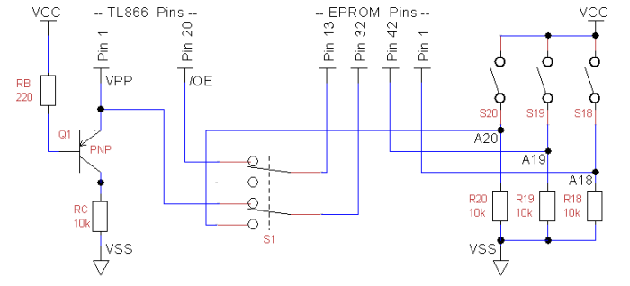
So with the extra circuitry, we now have our finished product, capable of allowing the TL866 to program 27C322’s, 160’s, 800’s, and 400’s.
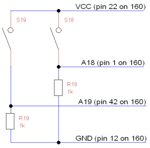
Standalone 27C160, 27C800, 27C400 Programming Adapter
This is an older design I made that only programs 27C160’s, 800’s, and 400’s. It’s a lot simpler to understand, and doesn’t require the need for a DPDT switch or PNP transistor.
In order to program the 160’s, we’ll need to reroute the pins on the 160 to match the pinout of the 27C4096, which the TL866 supports. Here’s the pinouts of each of the chips from their datasheets, and the rewiring you’ll need to do.
Pin 1 (A18) and pin 42 (A19) are not available on the 4096, so they will go to the switches that will turn the two address lines to 1’s or 0’s. Here’s a schematic of how you’ll need to connect them to switches using a pull-down resistor.
Simple enough, right?

It writes some of the chips but even tho they are blank sometimes it refuses to write. and gives this verification error. Pin detect and Check ID all disabled.
LikeLike