Well, it finally seems that I’ve arrived at the conclusion of my DMG Color journey!
My last attempt to fit a Game Boy Color inside of an original Game Boy (DMG) case was ultimately successful, but it was quite unorthodox. Cutting up the PCB and wiring everything manually was a huge task, and it came with some challenges to overcome as well. Not to mention, screwing the two halves back together without pinching any wires is a huge pain and something I don’t take any joy in doing, which is why it hasn’t been opened again since I finished the build. But, it had all the features I wanted to put into it, and I’ve already put many hours of playtime into it. But, every time I play it, I noticed how much lighter the actual console is – the LiPo inside wasn’t as heavy as the 4x AA batteries. And actually, since I didn’t incorporate load sharing into the battery charger, I found myself waiting for the battery to charge up when I wanted to play it. And, as it always does… the itch returned to make something fun and new. (Who even plays video games anyway?)
So I set out to make my own custom DMG-shaped PCBs to fit inside a DMG shell, and implement full Game Boy Color support. A true DMGC, redesigned from the ground-up, with a bunch of improvements and new features over my last build. Introducing the new Game Boy DMG Color:

Disclaimer
Before I go any further, please read this VERY important disclaimer, if you are thinking about making this yourself.
I made this project first and foremost for my own purposes. Nearly all of the features I have included are things I personally wanted. I have tried my hardest to make the project modular, if others would like to improve or change things easily, and I have also tried very hard to make the design somewhat less prone to potential errors during assembly (such as spacing out power pins on the FFC connectors). But in the end, every decision I made was for what I wanted the final product to be, with my skill level in mind.
Schematics, gerbers, and the BOM are provided in the various folders. If you choose to build this project yourself, be warned – this is a considerably advanced, and expensive build. You must be comfortable with the fact that you may lose or damage expensive components. You are 100% liable for any damage done to your property or yourself. I am not responsible for any damage or loss of property incurred while attempting this project, or after completion of the project – you alone accept all risk. While I am confident in this design, I cannot claim full compatibility with every system configuration. And there may be latent issues that have yet to crop up. I will update this repo if I encounter any, and if you see anything I may have missed, or some dubious design choice, feel free to ask questions or comment as such. Corrections are welcome. However, I will not obligate myself to providing tech support. You accept all risks and costs associated to this build if you choose to attempt it.

DO NOT attempt this project if you are uncomfortable or inexperienced with detailed electronics troubleshooting, or are not proficient in soldering! You will AT MINIMUM need to be proficient in drag soldering and hot air reflowing. If you have not gained proficiency in these soldering skills, DO NOT ATTEMPT THIS PROJECT.
(If you attempt the build, start with attempting to assemble DMGC-PWR-01. This is the toughest board to assemble, and it requires no donor components.)
Table of Contents
1. Overview
As I mentioned, this is an original creation – newly designed PCBs, with only some necessary components harvested from an original Game Boy and Game Boy Color (no hardware emulation – this project uses the original CPU). Here are the project goals:
- An original Game Boy aesthetic, using the original Game Boy shell and interface (link port, volume wheel, power switch, etc.), but with the capability of playing both Game Boy and Game Boy Color games.
- A nice, large IPS screen – the GBC Q5 XL IPS Backlight with OSD kit – with brightness and color palette control via the “navigation switch” housed where the contrast wheel used to be. (I will refer to the PCB attached to the Q5 screen as the “Q5 board”)
- A modernized, efficient switch mode power supply that can run off 4x AA batteries or input from the DC jack, just like the original DMG. Testing shows that playing with NiMH AA batteries can yield more than 18 hours of gameplay at normal settings (AKA, the way I normally play it – maximum brightness and headphones).
- Louder, warmer sound through a modern audio amplifier.
- The option for tactile switches for the face buttons – like the GBA SP.
- The option for backlit buttons, with multiple color modes and brightness control.
- No externally viewable case modifications, outside of trimming the DMG power switch cover for Game Boy Color game compatibility.
The code name for this project is DMGC. This console uses four PCBs, just as the original DMG model did – a CPU board (DMGC-CPU), display board (DMGC-IPS), power board (DMGC-PWR), and headphone board (DMGC-HDP). All circuit board assemblies have their own separate folders in the GitHub repository which contain detailed descriptions of operation, source files for schematics and board layouts (designed using Eagle), exported Gerber files, and some other relevant files.
Bill of Materials
The master BOM with every electronic component required for the four circuit boards is provided here in Excel format. Note that some parts may be out of stock at the links provided in the Excel document, but many can be found at alternate other retailers online, or have a proper substitute. Here is a saved cart from Mouser that contains all the parts in the BOM Excel, including some duplicates. Again, some parts might be out of stock, so double check to see what is missing, and consider ordering multiples of some parts.
The following is the high-level BOM for my specific build pictured above. Note that parts that deviate from the ones listed here (like different shell designs) might necessitate different fitment modifications, or end up being incompatible.
- Original Game Boy Color console
- U1 – CGB CPU (I used version B, I expect any revision except for E, which has a different pinout, will work)
- U2 – LH52256CVTXIZ – A replacement can be purchased here
- X1 – 8.388 MHz crystal oscillator
- EM10 – A replacement can be purchased here
- Original Game Boy DMG console
- VR1 – Volume dial
- SW1 – Power switch
- P1 – Cartridge connector
- EXT port
- DC jack
- Headphone board components (importantly the headphone jack)
- GBC Q5 XL IPS Backlight with OSD
- FunnyPlaying DMG Q5 IPS Lens (black)
- Custom designed 3D-printed IPS bracket (file located within the DMGC-IPS-01 folder on the GitHub repo)
- Game Boy DMG Shell – Factory A (Midnight Blue)
- Kitsch-Bent clear silicone DMG buttons
Buying from RGRS? Consider helping out some cool people with these referral links:
Or use one of these discount codes at checkout:
- Nataliethenerd
- B23N
- Tito
Note that the IPS kit I have listed is the easiest IPS kit to use that is compatible with this build. It includes an image centering feature, so you don’t need to fiddle with centering it manually in the shell. Other kits likely would not center nicely in the DMG shell! This kit works electrically, but requires you to center the image yourself. If you end up making some sort of 3D-printed bracket to support this screen, feel free to share it here.
Circuit Boards
For the circuit boards themselves, I have provided the zipped Gerbers and ordering details in each of the board folders above, as well as shared projects on PCBWay. For full disclosure, if you buy the PCBs from PCBWay, I will receive 10% of the total sale towards buying more boards from PCBWay. You can alternatively use these Gerbers at other PCB fabricators if you would like.
I also sell them on my Etsy store, so you don’t have to buy multiples!
2. DMGC-CPU-01


The image above of the assembled board is of v2.0, not the current revision of v2.2. The differences in appearance are minor, see below.
The CPU board houses the majority of the electronics in the DMGC. Parts harvested from the original GBC include the CPU, SRAM, and crystal oscillator. EM10 may be transferred as well, but a good enough replacement is included in the BOM if you need a new part. The power supply modifications, the new audio circuit, and a handful of omissions like the IR communication and some of the now-unnecessary LCD pins differentiate this build from the original GBC. But many connections and component values are pulled from the official GBC schematic (linked below).
Board Characteristics
The zipped folder on the Github repo contains all the gerber files for this board.
- Layers: 2
- Thickness: 1.2 mm
- Surface Finish: ENIG or HASL
- NOTE: When ordering PCBs, add this note to the order: “The file milling.gbr contains outlines for plated slots. Please add plated slots on the PCB according to this layer.”
HASL will work, but will potentially be more difficult for soldering fine-pitch parts like the CPU and FFC connector.
I sell this board on Etsy, so you don’t have to buy multiples from board fabricators.
You can atlernatively use the zipped folder at any board fabricator you like. You may also buy the board from PCBWay using this link (disclosure: I receive 10% of the sale value to go towards future PCB orders):
Customization Options
This section will briefly mention all of the different customization options you have on this board while assembling. More detail on implementing the options are in further sections.
- Maximum Volume: Increase R30 and R32 to decrease the maximum output volume. 100 kΩ will yield approximately the same volume as a stock GBC. Values below 20 kΩ are not recommended due to power draw considerations.
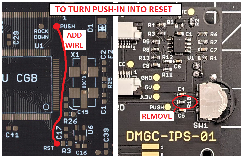
- Navigation Dial Push-in as Reset Button: Solder a wire from the PUSH pad to the RST pad. Make sure you do not populate R10 on the DMGC-IPS-01.
- Navigation Dial Rock Down as Reset Button: Solder a wire from the ROCK DOWN pad to the RST pad. Make sure you do not populate C5 on the DMGC-IPS-01.
Power Supply
The majority of the crucial power supply circuitry is on the PWR board, but the CPU board still has some portion of power supply interfacing.
NOTE: When assembling the DMGC, I highly recommend assembling the PWR board and the following components first. Then, power on the console with batteries or external supply without any other devices on the CPU board to make sure the PWR board is assembled correctly. Check with a multimeter or oscilloscope to make sure the 5 V and 3.3 V supplies are correct and steadily providing the correct voltage. If there is an error in assembly on the PWR board, the voltage could be too high and damage parts — like the CPU!

(I know the symbols for the fuses and filters are incorrect. I needed an 0603 package for the board and was too lazy to assign the parts the correct symbols. But I guess technically… they are all resistors in some form.)
- As mentioned on the main README, the DMGC uses the power switch to control the enable pin on the converters on the PWR board. Therefore, the battery voltage is always connected to the PWR board converter inputs. This way, system current does not pass through the switch, which can be dirty or oxidized and introduce unwanted voltage drops at higher currents.
- A downside of connecting the batteries directly to the input of the converter – as soon as the last battery completes the circuit by touching the terminals, the input capacitance is immediately charged up. This causes a considerably large inrush current – up to about 2 A by my measurements. In order to limit this inrush current, I utilize PTC1, a Polyswitch. This is a resettable overcurrent protection device. As current reaches 1 A, the resistance of the PTC will increase until power to the console is essentially cut off. For short bursts, like for the inrush current from the batteries, the resistance will quickly return to its normally low value. Nominal operation of the DMGC should only see currents up to 250 mA at worst cases – meaning the voltage drop across the PTC under normal operation will be negligible.
- Furthermore, because the batteries are always connected to at least some of the system, the current draw while the switch is off must be as small as possible to reduce the amount of quiescent current that would drain the batteries. Only capacitors and high impedance loads are therefore connected to the VCC line on the CPU and PWR boards.
- Because there is still a risk of the batteries being short circuited before reaching the PTC on the board, the positive battery terminal is immediately followed by a ~2.5 amp fuse to open the circuit if the batteries are accidentally short circuited. Also, F2 is in series with the output of the DC jack to protect from overcurrents if batteries aren’t being used to power the console.
- Pins 3 and 4 on the DC jack are normally closed when the AC adapter is not plugged in, and open when it is plugged in. This ensures the batteries and AC adapter cannot power the Game Boy simultaneously, and prevent accidental backfeeding into the opposing power source.
- Q1 is a P-channel FET used for reverse polarity protection. This is more efficient than a series diode because while the P-FET is conducting, there is a much smaller voltage drop than if a diode was being used. D1 is reverse polarity protection for the DC jack input, where efficiency is much less important than running on batteries.
- R1 connects to the 5 V rail when the power switch is turned off, ensuring quick discharge and reducing the chance of strange operation during a slower power down.
- U4 is a simple linear regulator for generating the 3.3 V supply necessary for the RAM and the CPU core. I considered using a SMPS instead, but the current requirements are so low, it seemed slightly overkill.
- The filters (EM6, 7, 8, and 10) are likely fine to exclude, but it doesn’t hurt to include them just in case some weird high frequency components have the potential to screw something up down the line. I don’t really have the capability (or desire) to properly test what effects removing them may have, but I suspect they’re mostly for FCC compliance.
- If the EM10 from the GBC donor board has a fifth pin in the middle, just bend it up so it doesn’t touch any of the nearby pads. It is an unused pin.
- Finally, there are five wires leading from the CPU board to the PWR board – VCC (battery voltage), SW (battery voltage after switch), DC (input from the DC jack), 5V (supply from the PWR board), and a GND reference. I also added test points for each of the three voltages as well for troubleshooting purposes.
Note: NiMH batteries that I have used have a shallower positive tab than normal alkaline AAs. This can cause poor contact with the battery contacts in the battery compartment. Keep the positive contact on the CPU board as close to the battery bay as possible, meaning install it at the very bottom of the mounting hole on the CPU board. If, when using NiMH batteries in the system, the power doesn’t turn on – try using alkalines or the DC jack input to check for operation. It might not be powering on due to poor contact of the NiMHs with the battery contacts on the CPU board or in the battery bay. Reseating the batteries can solve the issue.
FFC Connector
For this build, as mentioned, I’m using the GBC Q5 XL IPS Backlight with OSD kit. It comes with a separate circuit board to properly drive the IPS screen (which I’m henceforth calling the “Q5 board”). In order to determine which pins were necessary for the Q5 board, I looked at the cable connected to the board and noted which traces actually go somewhere. The pins in red are unused, the ones in blue are used. The pin names are from the GBC schematic. Some of the unused pins are used for other functions on the connector to connect to the IPS board.

- Pin 1 and 2 are connected to the output of the power switch. This is sent to the IPS board, which uses it for battery level detection to control the brightness of the power LED, and has a pad for connection to the OSD kit (after a voltage divider). As the kit is for the GBC, cutting the battery voltage in half simulates 2x AA batteries like the GBC uses.
- Pins 33 and 34 are used for GND. This just reduces the current through one individual pin on the FFC connector. Probably not necessary, but who knows. Maybe you’d want to put bluetooth or Wi-Fi or a media server on the front display board, I’m not your dad.
- Pins 38 and 39 are similarly doubled up for the 5 V supply. I wanted to keep some empty space around these pins to reduce the likelihood of shorting something to the power rail when soldering the FCC connector on, specifically the buttons (which are referenced to the 3.3 V supply in the CPU).
- Pins 41 to 48 are used for the face buttons.
- Pins 49 and 50 are for the speaker.
- TEST1 is used for GND on this cable, but I kept the ground connection to just a few pins to reduce the chance for ground loops between the CPU and IPS boards. But on the IPS board connector to the Q5 board, this TEST1 pin is connected to GND.
- Pin 4 connects to a test pad called PUSH. This pad connects to the rocker switch on the IPS board through the FFC, specifically the push-in function of the rocker switch. You can use this for all sorts of shenanigans if you want to try being clever with it.
- The CLS and LP pins aren’t used by this kit, but is by another kit that is potentially usable.
Audio Amplifier
The new audio driver on the CPU board is powered by the LM4853. This TI chip is perfectly suited for the Game Boy – it has stereo inputs and headphone outputs, and mono speaker output. Makes it quite easy to implement without extra circuitry shenanigans.
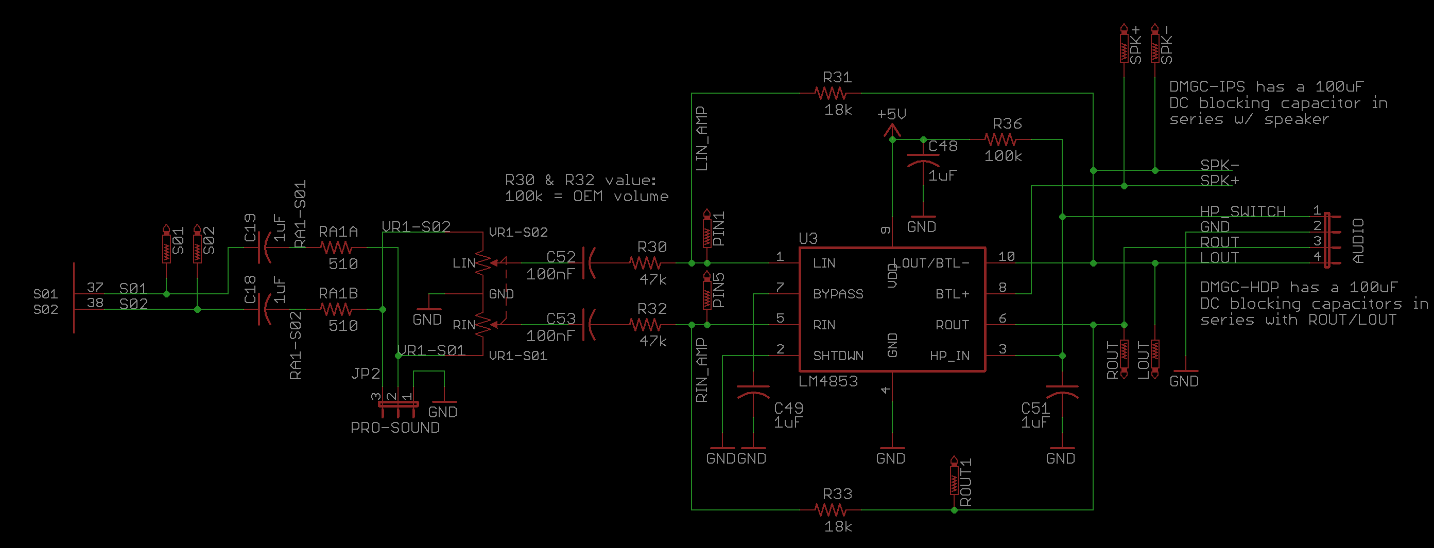
- The four outputs on the right are for the DMGC-HDP board. (This board has the DC blocking capacitors needed for the headphones)
- The headphone detect pin (HP_SWITCH) is connected to GND when the headphone jack is empty, and is pulled up to 5 V via R36 when headphones are inserted. This switches the output on the audio amplifier between the speakers and headphones. C51 is for debouncing the headphone detection.
- C18/C19 are DC blocking capacitors and RA1A/RA1B are current limiting resistors, so when the volume is turned all the way down, the S01 and S02 pins aren’t overloaded.
- C52/C53 are DC blocking capacitors so only the AC audio signal passes to the amplifier.
- The ratio of R30/R31 and R32/R33 set the amplification of the audio amp – increase R30 and R32 to decrease the output volume. 47 kΩ seemed to hit a sweet spot for my tastes for a gain of 0.38. This is louder than the original GBC, but not too loud that the audio quality is impacted. If you pick 100 kΩ you’ll get output comparable to the original GBC.
- The audio gain has quite a large effect on the power draw of the system when using the speaker. I did not do any tests with an audio gain greater than ~0.6. A sufficiently larger gain than this will drain batteries faster if the volume is turned up.
- The shutdown pin should be tied to GND to allow the amp to work. I made two different revisions that tied this to 5 V instead. Oops. (The output on the headphones will sound really quiet and the speaker won’t work if the chip is shutdown)
- The speaker output shouldn’t need a DC blocking capacitor, as the LM4853 outputs to the speaker as a bridge tied load (BTL). However, I found that if a DC blocking capacitor is not included, a strange issue is possible in specific situations. There’s a very brief moment when plugging the headphones in where the right output channel is shorted to ground (ring and sleeve are connected inside the jack). When this happens, the right output DC blocking cap is connected to GND, and causes a large surge of current from the power supply to charge it up. In my testing, this sometimes would cause a brownout, causing the power supply to shut off. So I have included a spot for one of these caps in series with the speaker on the IPS board.
- Added in version 2.0, opposite of the regular headphone outputs, are another set of audio outputs that are completely optional. These are denoted as “pre-pot audio,” and include a left, right, and ground connection. The left and right connect directly to the VR1-S01 and VR1-S02 nets, which allows you to grab the audio unfiltered, unamplified, right from the GBC CPU (through a protection resistor/capacitor combo). This is colloquailly known as the “pro-sound” mod, and is typically used in conjunction with a second audio jack. Audiophiles like to use this raw output with their audio equipment (note that using the pro-sound output as input to an external amplifier does not disable the speaker or headphones – the potentiometer still controls volume for those audio outputs). You could use this jack for headphones if you want (and it will disable the speaker), but it will always be one volume – about as loud as the original GBC at max volume. The audio coming out of these pins does sound incredibly clean – check out the recordings in the root folder. These outputs should make the system compatible with any pro-sound headphone boards, like this one.
CPU Reset
The last major change to the CPU board is the reset IC. I’ve replaced the original PST9135N with a TPS3840DL35. These chips pull the /RESET pin on the CPU low when the voltage supply drops below 3.5 V (/RESET set to low turns off the CPU). The TPS3840DL35 does the same thing. The reason this chip is included is to hold the CPU off while powering down so no random instructions are made while the game is turning off.
R3 and C17 introduces a time delay on the /RESET pin during start-up, to allow the rest of the power supplies to stabilize before letting the CPU operate. This is called a “power-on reset” circuit, and I used values that the original GBC schematic used. (The DMG, GBC, and GBA all use the same odd 18 ms time constant!)

Adding a Reset Button Functionality
Version 2.0 introduces a test pad labelled “RST” that connects directly to the /RESET pin. If this pin is pulled to GND, when it’s released it the system will reset back to the boot screen. If you wire this pad to a button that connects the pad to GND when pressed, you basically have added a reset button to your DMGC.
There are also pads near the FFC connector that are added labelled “PUSH” and “ROCK DOWN”. These connect to the rocker switch on the DMGC-IPS-01 board (version 2.0 and later). The PUSH pad becomes connected to GND when the rocker switch is pushed in and floats when not pressed (as long as you remove R10 on the DMGC-IPS-01 board). The ROCK_DOWN pad connects to GND when the rocker switch is rocked down, and floats when not pressed (as long as you remove C5 on the DMGC-IPS-01 board).
In a normal configuration, pushing in on the rocker switch will control the button LEDs, and rocking down will swap the Q5 color settings, but if you don’t want to use one of these features, then adding a wire from the PUSH or ROCK DOWN pad to RST pad will turn the rocker switch into a reset button for the system for that specific action and replace its normal function.
CAUTION: Remember to remove R10 or C5 on the IPS board if you plan to use this feature!!!

3. DMGC-IPS-01


The image above is of v2.0, not the current revision of v2.1. The differences are very minor, see below.
The IPS board is in the front of the DMG shell. This holds the IPS screen kit (and has pads for interfacing with it), has the dimmable power LED, button inputs along with pads for optional LEDs, a navigation switch on the side for changing settings on the IPS screen and the backlit buttons, and the speaker.
Board Characteristics
The zipped folder on the Github repo contains all the gerber files for this board.
- Layers: 2
- Thickness: 1.2 mm
- Surface Finish: ENIG
ENIG is required for reliable button press detection.
I sell this board on Etsy, so you don’t have to buy multiples from board fabricators.
You can atlernatively use the zipped folder at any board fabricator you like. You may also buy the board from PCBWay using this link (disclosure: I receive 10% of the sale value to go towards future PCB orders):
Customization Options
This section will briefly mention all of the different customization options you have on this board while assembling. More detail on implementing the options are in further sections.
- Tactile Buttons: Pads are included for tactile switches (clicky buttons like the GBA SP) to be installed on the board. If using tactile buttons, HASL can be used as the surface finish.
- Power LED Brightness: Increase the value of R1 to decrease the brightness of the power LED during normal battery levels. Increase the value of R2 to decrease the brightness of the power LED during low battery levels. It is suggested to try changing resistances in ~5 kΩ increments.
- RGB Backlit Buttons: If you would like RGB LEDs behind the buttons, you must install LED10-LED17, R9, C2, and U2.
- Always-on Single Color Backlit Buttons: If you only want backlit buttons with non-controllable LEDs, you can omit R9, C2, and U2. You must install R22-R29, as well as the discrete 0603 LEDs as detailed in a below section.
- No Button LEDs: You do not need to populate LED10-LED17, R9, R22-R29, C2, or U2.
- Alternate OSD Controls: You don’t need to use the SEL, A, and B pads at the top of the board for the OSD controls. You can alternatively use the button pads in the middle of the board instead.
- Navigation Dial Push-in as Reset Button: Do not populate R10. See DMGC-CPU-01 notes for further instructions.
- Navigation Dial Rock Down as Reset Button: Do not populate C5. See DMGC-CPU-01 notes for further instructions.
FFC Connectors
There are two FFC connectors on the board – one to take the input from the CPU board, the other is for the Q5 board to connect to. The former is detailed in the CPU board section, and the latter simply omits a few pins to connect to the Q5 board, such as the speaker and button inputs. Notably, the connector going to the CPU board must be reversed due to the FFC cable connecting it to the CPU board.

Speaker
I mentioned that a DC blocking capacitor needs to be included in series with the speaker output. That’s what C3 is for, a 100 uF capacitor. There are two capacitors called out as C3 – a space for an aluminum electrolytic capacitor, and one for an electrolytic tantalum. If you install the through-hole electrolytic, bend it down into the notch on the board. I have a ton of aluminums and they’re cheaper, so that’s the one I used. The speaker itself is an aftermarket FunnyPlaying model.

Power LED and Dimming Circuit
The power LED is a standard 3mm red LED. For low power detection, I used a simple Schmitt trigger circuit.
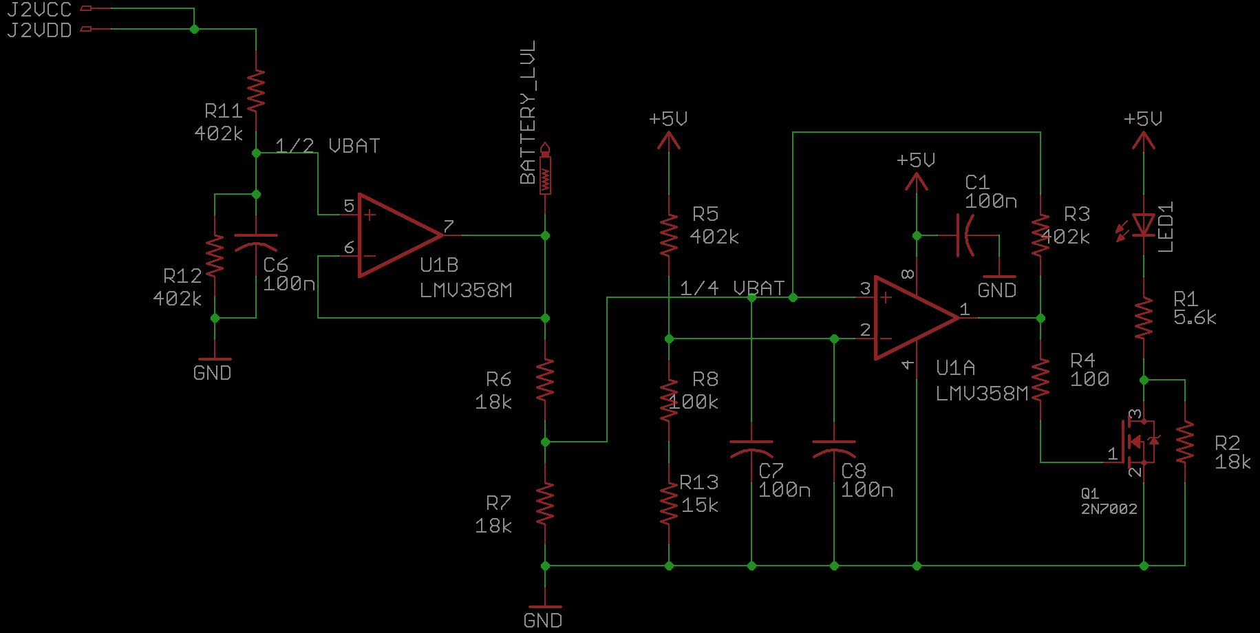
When the power switch on the CPU board is turned on, the input to the buffer (U1B) is half the battery voltage, from the voltage divider made from R11 and R12 (C6 is for noise filtering purposes). This output is connected to the Q5 board’s BATT solder pad for battery level indication. Since the Q5 kit expects a GBC battery voltage, which uses 2x AA batteries, cutting the 4x AA battery voltage in half will scale it properly. The Q5 board itself uses a voltage divider for scaling the battery voltage, so the voltage on the BATT pad must be from a low impedance source so as not to ruin the scaling factor – therefore, it must come off of the op-amp output itself, rather than the voltage divider.
The ½ battery voltage is then cut in half again via the voltage divider made by R6 and R7. The ¼ battery voltage is compared with the inverting input on the other half of U1. R3 provides hysteresis on the comparator circuit (i.e. Schmitt trigger), and C7 and C8 are for noise filtering (can likely be omitted). When the combined voltage of the 4x AAs drops below ~4.35 V, the battery level is considered low and the LED will noticeably dim. My testing came up with this voltage as approximately 30 to 45 minutes of playtime left if at max brightness with headphones in, testing from fully charged batteries.
The output of the op-amp is set at 5 V when the battery level is high, which turns on Q1; it is driven to GND when the battery level is low, which turns Q1 off. Therefore, the brightness of the LED during normal power is dictated only by the resistance of R1. When the combined battery voltage drops below the low battery threshold, R2 is placed in series with the LED as well, which dims the LED. I played around with these values to find ones that didn’t burn my retinas for normal brightness, and produced a noticeably dimmed power LED when the low voltage detection is tripped.
If you want to decrease the brightness of the LED, increase resistance values of R1 and/or R2 (increase R1 to decrease brightness for both normal and low battery levels, R2 to decrease brightness for only low battery level).
Navigation Switch
This takes place where the contrast wheel used to be. On the Q5 board, there are two capacitive touch sensors – one for changing brightness, one for changing the color palette. Instead of using the touch sensors in the DMGC, the navigation switch will toggle these inputs by connecting a series capacitance to ground to simulate a touch. This also has the benefit of not having to modify the driver board in any way, and instead just requiring soldered wires to the board where capacitive sensors were connected.

Rocking up on the dial will toggle the brightness setting, rocking it down will toggle the color palette setting. Rocking up and holding it will toggle the battery level display on the screen, and rocking it down and holding it will toggle the pixel grid. Pushing in on the switch grounds the ATTINY85’s PB3 pin (which is pulled up externally to 3.3V), if installed. Using the code I provide above, pushing in will advance to the next color of the button LEDs, and holding it while pressing left or right on the D-pad will change the brightness of the LEDs.
Bridging the solder pad labeled “NEOPIXEL DISABLE” will ground the navigation switch push function, which will prevent the LEDs from turning on at all. You can ignore it if you aren’t using Neopixels at all.
Adding Reset Button Functionality
- If you are using the push function of the navigation switch to reset the console instead of controlling the button LEDs (see more info on the CPU README), then make sure to remove R10. You will not have the ability to control Neopixel LEDs with this change (without other code/hardware modifications).
- If you are using the rock down function of the navigation switch to reset the console instead of controlling the Q5 palette setting (see more info on the CPU README), then make sure to remove C5. You will not have the ability to use the palette swap function of the Q5 kit with this change (but who really cares, amirite?)


Q5 Board Pads
There are six test points at the top of the IPS board for short wires to connect to the Q5 board. The Q5 board includes pads for the select, B, and A buttons for navigation in the OSD. There’s also a battery pad, which is for measuring the battery life, as mentioned. And finally, there are two pads for brightness control and color palette swapping, which connect to the capacitive touch sensor inputs on the Q5 board. Before installation, stripped wires should be soldered to these corresponding pads on the Q5 board, so they may be soldered to the IPS board after assembly.

Button LEDs and ATTINY85
One popular feature for Game Boy mods are backlit buttons. On the front PCB I included spaces for eight WS2812B-2020 RGB LEDs. These are controlled via an ATTINY85 with the Adafruit NeoPixel library. You can program the ATTINY in any number of ways, but I added pads for kinked header pins to hopefully make it a bit easier. You can find the code in the github repo here.

Note that if you do not wish to include LEDs for the buttons, you don’t need to populate any of the parts shown in this screenshot.
There are nine color settings – red, orange, yellow, green, cyan, blue, purple, white, and off. These settings can be changed in the code (or additional settings could be appended) by changing the RGB values in the arrays. Pushing in on the navigation switch will toggle between these settings. Pushing and holding it in, and then pressing left or right will change the brightness of the LEDs. The settings are saved every time the brightness or color is changed, and will be reloaded when turning on the Game Boy. This feature was inspired by NiceMitch’s RGB LED flex PCB for GBC.
Code for the ATTINY85 is included here, however because I wrote this months ago (and forgot to comment it sufficiently…) I have forgotten how some of the code actually works. There’s certainly room for improvement (and some really dumb inclusions). But there is a nice startup effect to match the Game Boy Color boot sequence that a friend (jokingly) suggested I include. Are you happy, Mike?
NOTE: If you are programming the ATTINY after it is already soldered to the IPS board, be sure to disconnect the ribbon cable going to the CPU board and the ribbon cable going to the Q5 kit.
If you hold the navigation switch in as you turn on the console, the LEDs will be disabled until power is cycled. (This is probably more for my benefit as I used it while testing very discharged batteries to skip the start-up LED sequence)
Always-on discrete LEDs are also an option – an 0603 LED will fit on half of the 4-pin RGB LED pads, from VDD to DO. The pads for this are indicated by the arrows. The picture below shows which pads to use for discrete LEDs (view of the D-pad) – the A indicates the anode of the diode. There are spaces for a resistor for each LED on the back of the board (R22 to R29). If you’re using the RGB LEDs, or no LEDs at all, the resistors aren’t necessary.

Oh, and when you solder the LEDs on, I recommend taping off the button contacts to make sure you don’t get solder on them. It won’t damage them to the point of non-function, but it can potentially reduce their useful lifetime and accurate detection depending on the severity. (But more importantly, it’s not A E S T H E T I C)

Optional Tactile Buttons
Version 2.0 introduced the option for including tactile switches for the buttons, much like the Game Boy Advance SP had. I did not however bother to add switches for start and select, due to the mismatched geometry (and you don’t press them that often). If you do not wish to use these kinds of buttons, the button contacts are still set up to act just like the regular set up with membranes.

In this image, tactile switches are on the left, and pads for simple membranes are on the right. Either method for button presses works perfectly fine.
If you’re doing tactile switches on the start and select buttons, you should do a trace cut as indicated where the white lines are pointing. If you don’t, the membranes can still activate the start/select buttons on the exposed area without actuating the tactile switch. You may also want to tape over the exposed copper not underneath the switches while soldering them on to avoid getting stray solder on the exposed traces and ruin the A E S T H E T I C.

Q5 IPS Screen Bracket
I designed a bracket for holding the screen in place. This is placed between the screen and the DMGC-IPS-01 board. The model is available for download here.
It is similar to Funnyplaying’s Retro Pixel DMG kit model.

4. DMGC-PWR-01


The PWR board has gone through a few iterations. Because the system will run with 4x AA batteries or the DC jack input, the range of input voltages is relatively wide – anywhere between ~4 V up to ~8 V, plus margin. The output voltage must be maintained at 5 V. The logical choice would be a buck-boost converter. Thus, the DMGC-PWR-01 utilizes the TPS630702 (or TPS63070 or TPS630701) – a buck-boost converter with only a few external parts required for operation, that accepts anywhere between 2 V and 16 V to produce a 5 V output.
This board is likely the most complex part of the build. I spent a lot of time tuning the circuit to produce the exact results I wanted with ample protection downstream of the converters.
Board Characteristics
The zipped folder on the Github repo contains all the gerber files for this board.
- Layers: 2
- Thickness: 1.2 mm
- Surface Finish: ENIG or HASL
HASL is acceptable, but might introduce a bit of difficulty soldering the QFN chip owing to the possibly uneven surface compared to an ENIG finish.
I sell this board on Etsy, so you don’t have to buy multiples from board fabricators.
You can atlernatively use the zipped folder at any board fabricator you like. You may also buy the board from PCBWay using this link (disclosure: I receive 10% of the sale value to go towards future PCB orders):
Schematic and CPU Board Interfacing
There are five wires that connect to the CPU board power supply circuitry. Pin 1 is the GND reference and pin 2 is the 5 V output from the PWR board. Pin 4, VCC, is the input voltage, which is always powered from the CPU board. SW is the output of half the power switch on the CPU board – connected to VCC when on, floating when off (ultimately tied to GND through R16 on the PWR board). On the CPU board, pin 3 is connected to the DC jack output, but on this board I connect this to VCC as well, so that either batteries or the DC jack will power this board. A different revision might utilize the DC jack for something else, such as charging a LiPo battery, which is why I left these pins separate.

The battery voltage, VCC, is applied to the buck-boost input voltage pin, without routing through the power switch on the CPU. Instead, the power switch controls the buck-boost converter’s enable pin through a load switch circuit.
Buck-Boost Converter
U2 can be TPS63070, TPS630701, or TPS630702. TPS630701 is a fixed 5 V buck-boost, while the other two have adjustable output via a voltage divider. The only difference between TPS63070 and TPS630702 is that the latter has an output discharge function – when the output is disabled, a low impedance (~200 Ω) is connected to the rail internally to quickly discharge the output capacitors. If you have a choice, I would recommend using the TPS630702 over the other two, and the TPS630701 over the TPS63070 just because it’s a bit more convenient (and foolproof) to use the fixed output version of the chip. But any three of them will work perfectly fine. They don’t like to be in stock very often from what I’ve seen – check stocks on octopart.com. I have been lucky and found a few random instances of Digikey or Mouser getting in a handful of the chips (or, more likely, finding extra parts lying around in their warehouses). At the time of writing (September 2022), it appears Digikey, LCSC, and Texas Instruments themselves have some available for purchase (Mouser reports they will get them in October 2022).
Check this octopart link if you’re having problems finding one: https://octopart.com/search?q=tps63070¤cy=USD&specs=0
The bottom third of the schematic is the entire buck-boost stage. I followed the TPS63070 datasheet for choosing values of the input and output capacitance, the inductor, and the feedback resistors. R8 and R9 set up a voltage divider for setting the output of the adjustable TPS630702 or TPS63070 – if the TPS630701 is used instead, which is the 5 V fixed output version, then R8 should be short circuited and R9 can be removed. If you leave R8 and R9 at the values they are with the fixed 5 V chip, the output will shoot up to ~11V. I strongly recommend testing this power supply board separately from the rest of the system to ensure the 5 V output is correct and steady, without frying anything else downstream.
The buck-boost chip is activated when the EN pin is higher than 800 mV (there is an internal ~70 microsecond delay before activation after this voltage is reached). This pin is controlled by the PSU_EN net, which is influenced by two chips – U3 (overvoltage protection) and U1 (undervoltage detection). If no errors are detected in the power supply, then PSU_EN will pull up to VCC_LATCH and activate U2. If either an overvoltage on the 5 V line or an undervoltage on the battery supply is detected, the PSU_EN net is pulled to GND and latched off until the power switch is cycled. R5, R12, and R13 set up voltage dividers that ensure if the EN pin passes 800 mV, the gate-source voltage on Q2 will be at least 2.4 V, meaning the latching circuit will be set up before the 5 V supply is generated (VGSth of Q2 is ~2.1 V, max). R13 also ensures the EN pin is pulled to GND when the power switch is turned off. Detailed operation on the PSU_EN net can be found below.
F1 is a 1 A fuse on the 5 V output, which in hindsight is probably overkill, since the CPU board has protections that will likely always trip first (the 1 A PTC specifically). When testing the PWR board, I shorted the 5 V supply to GND to see if the fuse would pop, and the PTC opened up first every time I tried. But, I have plenty of 1 A fuses lying around, so there’s little reason not to include it just in case, since the TPS63070 chips can output up to 3.6 A. A fuse could prevent a feed-the-fault type of error, however rare that scenario likely is.
Overvoltage Protection
Onto the protection circuitry – let’s get the easy one out of the way first. U3 is a TPS3702 IC. This chip monitors the 5 V output on the SENSE pin. If it’s above a certain value, the output on the OV pin will be pulled low. Otherwise, OV is left floating (it’s an open-drain output), so it doesn’t affect the output of the PSU_EN net during normal operation.
The specific part I have chosen is the TPS3702CX50. With the SET pin tied to GND, this sets the overvoltage threshold to 5.45 V. If the supply ever passes this point, then the overvoltage pin will pull PSU_EN low, and the latching circuit will keep it off until the power switch is cycled.
The overvoltage protection is likely overkill as well, as long as the buck-boost circuit is set up correctly and soldered properly. Since the adjustable TPS63070 chips measure the feedback through the FB pin, it will maintain the 5 V as long as no solder bridges or poor solder connections cause the wrong voltage to be measured by the chip (assuming the rest of the circuit is set up properly). You can omit U3, C9, and C10 to remove the overvoltage detection without impacting the operation of rest of the circuit.
Undervoltage Detection
U1 is a TPS3840 chip which monitors the voltage on the batteries via the VDD pin. When it detects the voltage has gone below a specific threshold, the /RESET pin is pulled low. This output is open-drain, so it does not affect the PSU_EN net while not in an error state.
The specific part I chose was the TPS3840DL35. The DL indicates the /RESET is an active-low open-drain output. (PL would indicate active-low push-pull output, PH would indicate active-high push-pull, both of which aren’t suitable for my specific application). The threshold voltage is determined by the last two numbers, which for my selection is 35 for 3.5 V. I chose this threshold based on the guidelines from this application note from Energizer. This documentation recommends using a voltage cutoff of ~75% of nominal voltage for a pack of NiMH AA batteries (what I will most commonly be using in my personal console). Nominal voltage of a NiMH AA battery is 1.2 V, so for four of them in series, the 75% level is 3.6 V. So the 3.5 V cutoff is close enough, and as a bonus, it’s a part used on the CPU board already.
The VDD pin of U1 isn’t directly powered by the battery voltage. C1 and R7 on the battery voltage filter out any fast power supply transients. I found that during the start-up sequence, the loads on the 5 V supply will draw a considerable amount of current from the batteries, causing their voltage to dip about a volt max (this is normal, and the PTC on the CPU board does not drop the supply more than a few tens of millivolts). Furthermore, loud audio can introduce kHz range ripple on the battery voltage when their charge is low, so the low pass filter will smooth that out. It’s not important for undervoltage lockout to occur immediately after the 3.5 V threhold is passed during a transient event, so this doesn’t negatively impact performance or protection while the console is being used. Also, the current draw of the TPS3840 is less than a microamp, so the voltage drop across R7 is negligible and it also won’t have any perceptible impact to battery life despite always being connected to the batteries.
The CT pin on this chip introduces a delayed start function. Adding a 1 uF capacitor to this pin will cause the /RESET output to be held low for approximately 620 milliseconds no matter what the supply voltage is. This is really only useful in the event you put the batteries in while the power switch is already on, because the delay only applies the first time power is applied to the chip. The wait period lets all the input capacitors charge up sufficiently and allows enough time for the input undervoltage latch to be set up before trying to generate the 5 V supply.
You might be asking – why am I including external input undervoltage detection on this board? Can’t you just put a voltage divider on the enable pin of U2? Well…
Latching Circuit
The original design of the PWR board had a funny problem, and didn’t include the undervoltage lockout chip or latching circuitry. When the buck-boost enable pin was pulled low to disable the output once the batteries discharged enough, everything would turn off and thus remove the load from the batteries. When the current draw out of the batteries suddenly dropped to almost nothing, the battery voltage would rise back up, as expected. Unfortunately, this voltage would soon re-enable the buck-boost chip, starting up the 5 V supply. But… that would increase the load on the batteries, the voltage would drop below the enable pin threshold, and the system would shut off again. And that cycle would repeat. A bootloop! Not the graceful death the original Game Boy experienced when the batteries ran out of juice.
So in order to fix this, I introduced the undervoltage detection chip along with a latching circuit, so that as soon as the batteries died the first time, the system would keep itself shut off until the power switch was cycled. I found this strategy in this very helpful application note from Texas Instruments. (You know, Texas Instruments should have sponsored this project, because I sure do use a lot of their parts)
The latching circuit consists of Q1 through Q4 and R1 through R4. You can read the application note for the full series of events, but basically turning on Q2 with a sufficient gate-source voltage sets up the latch. The next time the gate of Q2 (the PSU_EN net) is pulled to GND by the /RESET pin, Q4 is turned on to conduct and the /MR pin (master reset) is also pulled low. On the TPS3840, whenever /MR is low, /RESET will also automatically be pulled low no matter if VCC is above or below the undervoltage trip point. So even if the voltage rises back up above the trip limit, /RESET will keep Q4 conducting, which keeps /MR low as well. So the only way to reset the whole thing is to turn the power switch off and reset the latch.
Load Switch
VCC is applied to the latching circuit through a load switch circuit, rather than the power switch directly. The power switch, which is connected to the SW net, controls the gate-source voltage of Q5, an N-channel FET. R15 and C11 set up an RC delay for switch debouncing, and R16 is a pull-down resistor for when the power switch is turned off. R14 is a pull-up resistor that keeps Q6, a P-channel FET, off whenever Q5 is off. When the power switch is turned on, Q5 conducts and pulls the gate of Q6 to GND. This allows the battery voltage VCC to turn on the latching circuit. Furthermore, if PSU_EN is not being pulled to GND by the supervisory ICs (if the battery voltage is higher than 3.5 V), then the enable pin of the buck-boost will pass the 800 mV threshold needed to turn on the 5 V supply (after a built-in 70 microsecond delay).
The benefit to using a load switch instead of the power switch directly is the contact resistance of the 30+ year old power switches is no longer a factor in operation. One common issue in old Game Boys is a voltage drop across a dirty power switch, because the entire system current flows through the switch. Sometimes, if the switch is particularly oxidized or dirty, the entire Game Boy could fail to turn on. Instead of having to clean out a power switch, a non-trivial task (especially for a DMG), a dirty power switch will still be able to properly control Q5, as long as contact resistance isn’t higher than like, 100 kΩ. (And in that case, increase R16 to like 1 MΩ, and you might be ok!)
5. DMGC-HDP-01

The image above is of v2.0, not the current revision of v2.1. The differences are very minor, see below.
This little board is quite simple. You can transplant all of the parts from the original DMG headphone board to this one. This board also uses an original DMG headphone jack. Modifications to the circuit would be required to use an off-the-shelf jack.
Board Characteristics
The zipped folder on the Github repo contains all the gerber files for this board.
- Layers: 2
- Thickness: 1.2 mm
- Surface Finish: HASL
- NOTE: When ordering PCBs, add this note to the order: “The file milling.gbr contains outlines for plated slots. Please add plated slots on the PCB according to this layer.”
I sell this board on Etsy, so you don’t have to buy multiples from board fabricators.
You can atlernatively use the zipped folder at any board fabricator you like. You may also buy the board from PCBWay using this link (disclosure: I receive 10% of the sale value to go towards future PCB orders):
Circuit Overview

On the top of the board: pin 1 is the left output, pin 2 is the right output, pin 3 is the GND reference, and pin 4 is the headphone detect pin which is normally connected to GND through the headphone jack (when headphones are placed in the jack, pin 4 will be disconnected from GND).
R1 and R2 are included to pull down the negative sides of the DC blocking capacitors C1 and C2 when headphones are not connected – without them, the outputs would be floating. This will prevent inrush current during headphone insertion, which I have seen cause issues with the LM4853 in the past.
On v2.1, C1 and C2 can be replaced with tantalum electrolytic capacitors if you would like – the pads are for size 1411 (3528 metric).
Using the Original DMG Headphone Board
You can easily use the original DMG board instead of ordering this one, just be sure to put 1 kΩ resistors from the right output and left output to ground to prevent the inrush current issue.

6. Final Assembly
Now that I’ve finally discussed all the boards in detail, here are some pictures of the assembly process.
I highly recommend reading the information in the Troubleshooting and Testing folder in the repo. In it, I detail the testing procedure that I follow before fully assembling a DMGC. It is far easier to do this than to have to disassemble things when something doesn’t work.
Here are some pictures of the assembly process after testing the functionality of all the boards separately. Detailed images of the circuit boards alone are shown in their respective folders. These pictures are of a previous revision, v1.2, but the process remains the same. You may notice some minor cosmetic differences in these pictures from the current revision boards.
First, I started with the back half of the DMG shell. The PWR board needs five ~2.25″ wires that wrap around the screw post on the side of the shell. In addition to the PWR board connections, the HDP board needs four ~2.6″ wires. Also, the flat flex cable (FFC) should be inserted into the CPU board first, because the connector will be inaccessible after screwing the CPU board in the shell. After I soldered all the wires between the three boards and secured the FFC, I placed the assembly in the shell, and secured it with the proper screws. I put a game in the cartridge slot to keep the CPU board in place easier while assembling.

Before placing the power switch cover in, I cut a notch in it so that it wouldn’t prevent Game Boy Color games from being played in the system. In the left picture below I’m using Game Boy games, and in the right picture I’m using Game Boy Color. And you can see that the power switch is blocked from turning on by the GBC cartridge for the original model.

After the back half was done, I prepared the Q5 board solder pads. I cut six 30 gauge wire segments and soldered them on the brightness, palette, battery, and OSD input pads. These will be soldered to the rear of the IPS board after installed.

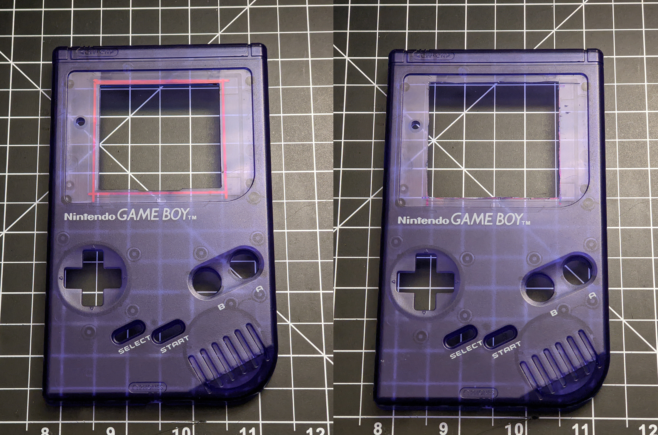
For the top half of the shell, as per instructions on a similar DMG IPS kit that uses the Q5 screen, I very carefully cut ~1 mm of plastic around the border of the viewing port, and trimmed any extra plastic to make the surface underneath the lens smooth (there are “IPS ready” shells that should not require this cut). I used a black paint marker to color in the edges of the newly cut plastic, so they would not be visible at an angle. And I trimmed two posts off of the shell so the screen would fit flush against it.
Then I installed the front lens, and placed the screen, backed with the 3D printed bracket, into the front half of the shell. I made sure to clean up any stray fingerprints or dust while assembling this part. Once the bracket was placed and flush with the shell, I put the buttons in and placed the IPS board over top, slid the Q5 screen FFC into the connector on the PCB (making sure it fit without any added stress on any connections), and secured it all in place. Then I very carefully soldered the wires from the Q5 board onto the appropriate pads on the IPS board – making sure not to melt any plastic on the shell.

If you installed the 7-pin headers for programming the ATTINY easier, you might want to tape off the headers with kapton tape. If everything is installed correctly, these shouldn’t interfere with anything on the CPU board after the halves are screwed together (C47 is the closest component), but you may want to consider it anyway.

After that, it was just a matter of connecting the FFC from the CPU to the IPS board, tucking it under the boards ensuring no kinks or sharp bends, and screwing it together. Once assembled, I opened the OSD menu for the IPS kit (Select + A + B) and changed the vertical and horizontal offsets (my values were 78 and 29, respectively) to center the image on the screen. The image centering function is one of the biggest reasons I chose this IPS kit.
Next to an original DMG… one can really see the improvements!

Auxiliary Controls
Other than the regular operation of the face buttons, the build comes with some extra button functions!
Q5 XL IPS Backlight with OSD
- Select + A + B: Open the OSD menu
- Select + A: Enter
- Select + B: Exit
- A: Increase
- B: Decrease
Navigation Switch
- Rock up: Advance screen brightness setting
- Rock up/Hold: Toggle on-screen battery indicator
- Rock down: Advance screen color pallete setting
- Rock down/Hold: Toggle on-screen pixel grid
- Push in: Toggle button LED color setting
- Push in/Hold + D-pad Left: Decrease button LED brightness
- Push in/Hold + D-Pad Right: Increase button LED brightness
- Push in/Hold when turning on power switch: Disable LEDs until another power cycle
Power Draw Measurements
For these estimates, battery life is calculated using four eneloop pro NiMH AA batteries (total of ~11800 mWh). Keep in mind that these are very rough estimates. I tried to be conservative in the power draw measurements, so hopefully these numbers represent a mostly worst case. Actual playtime will vary due to a variety of factors – changes in efficiency and performance as the battery voltage changes, differences in game audio, etc.
I measured the power draws using a MiniWare MDP-XP Mini Digital Power Supply, and estimated the average power draw shown on the display (I tried to bias towards a higher value). Input voltage was set to 4.4 V, just above the point where the power LED dims. I tested with the Legend of Zelda: Link’s Awakening, letting the game sit on the title screen after the intro cinematic, where sound is relatively loud and the screen is mostly white. The audio gain on the test console is set to ~0.38 (see CPU board for more detail on this gain value – a higher gain can greatly impact power draw at high volumes out of the speaker).
| Test Criteria | Power Draw | Estimated Battery Life |
|---|---|---|
| IPS max brightness, NeoPixel LEDs max brightness (white), speaker volume 100%, Everdrive X5 | 1150 mW | 10.3 hr |
| IPS max brightness, NeoPixel LEDs off, speaker volume 100%, Everdrive X5 | 900 mW | 13.1 hr |
| IPS max brightness, NeoPixel LEDs off, speaker volume 100%, original cartridge | 750 mW | 15.7 hr |
| IPS max brightness, NeoPixel LEDs off, headphones, Everdrive X5 | 725 mW | 16.3 hr |
| IPS max brightness, NeoPixel LEDs off, headphones, original cartridge | 650 mW | 18.2 hr |
| IPS min brightness, NeoPixel LEDs off, headphones, original cartridge | 475 mW | 24.8 hr |
Note: If powering through the DC jack instead of batteries, an OEM adapter may not be able to supply enough power to the DMGC at maximum settings. Furthermore, cables like these will require at least ~200 mA output from the USB port for reliable operation at all settings. (USB 1.0 and 2.0 are likely not sufficient for higher loads, such as with the button LEDs on)
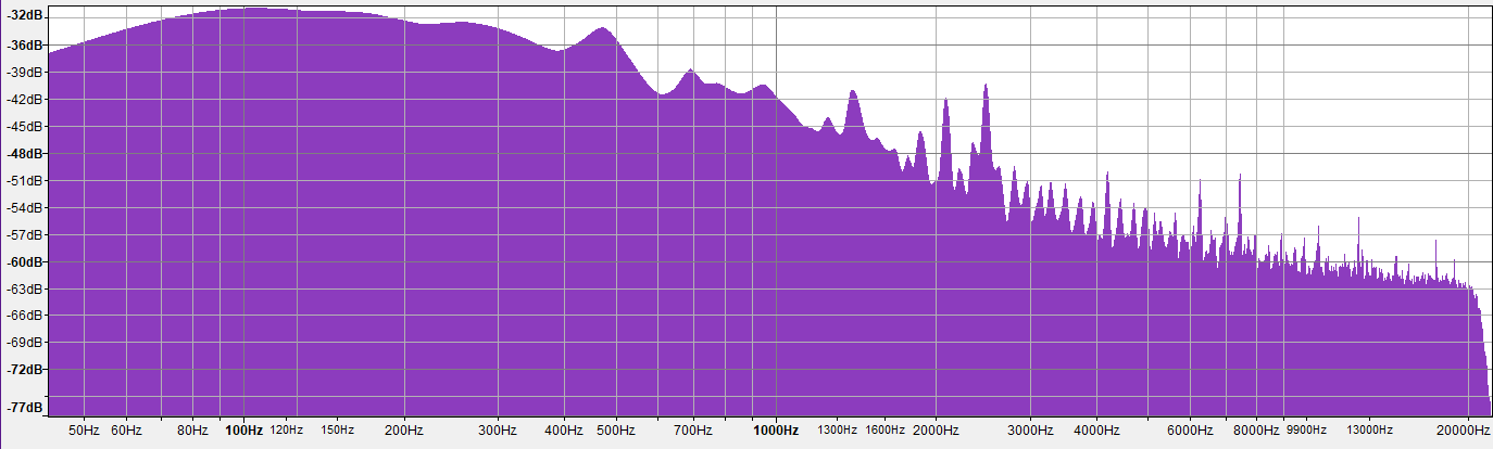
Audio Recordings and Spectrum
I mentioned the sound of the DMGC is “warmer” than an original GBC – it’s bassier with less buzzing background noise (owing mostly to the modernized power supply). I connected the headphone jack to my computer’s microphone input, and used Audacity to obtain line out recordings. Then I graphed the spectrum using Audacity’s “plot spectrum” analysis tool. You can see the larger gain at the lower frequencies in the spectrum plot of the DMGC. I also took some recordings of the pro-sound output as well – it’s even cleaner than from the amplifier. I’m not an audiophile, but I’m pretty sure the DMGC all-around sounds nicer, at least through headphones. Listen for yourself! (GitHub only allows for video files to be embedded, MP3 files are provided above)
Original GBC Audio
The background buzz is extremely noticeable in this clip, especially during quiet parts.
DMGC Audio
The silent sections are quite quiet on the DMGC!
DMGC Audio (Pro-sound)
Using the pro-sound outputs makes it even cleaner.
Original GBC Audio Spectrum

DMGC Audio Spectrum

DMGC Audio (Pro-sound) Spectrum
7. Conclusion
What an absolute marathon of a project. But boy, I am glad I was able to implement all of the features I wanted to in a slick package with custom-built PCBs. This truly has been my passion project for 2022 – I put hundreds, if not thousands of hours fine-tuning and exhaustively testing everything I could think of, and hundreds of dollars into prototyping builds! There were times I was ready to just set the project aside for other things, but I’m so glad I powered through it in the end. And I am so happy I’m able to share it with other Game Boy enthusiasts out there. I play this Game Boy nearly every day now, sometimes I just like to turn it on and see the buttons light up in the GBC start-up pattern! This project came out better than I could have ever hoped it would. And I hope you all enjoy the project as much as I do.

Possible Additions and Changes
Want to improve this project? Maybe try one of these things (because I probably won’t):
- This console uses 4x AAs instead of a single rechargeable battery in order to maintain the feel and weight of the original DMG model, but an obvious change to the build is to utilize a LiPo battery with proper battery management. The DC jack could be repurposed to charge the battery instead. With the advent of affordable rechargeable AAs, the appeal of the AC adapter is diminished, so this would be a good repurposing. However, the maximum output current of most DMG AC adapters is rated for ~200mA at ~6V, so charging would be considerably slower than, say, fast USB-C charging.
- Restoring the IR functionality of the GBC could also be done, as there is ample space for it on the circuit board and shell – I just do not trust myself with forming plastic to look nice, and it wasn’t at all an important part of the build for me.
- Finding aftermarket equivalents for all the different required DMG parts would be ideal, instead of using a (hopefully broken) DMG for a donor console. For my personal build, I used original DMG components because I had a damaged console lying around, but you can easily find DMG-style volume wheels and cartridge connectors online. The tricky parts are as follows:
- A GBC EXT port can be used in place of the DMG one (but would look kind of weird in the DMG EXT hole in the shell).
- There are a few power switches I’ve ordered to try out in place of the DMG one, but I haven’t gotten around to testing them yet. There’s no one fully drop-in replacement that I’ve found, though, so it would require circuit modifications.
- I haven’t been able to locate a headphone jack exactly the same as the DMG one, but the circuit could be adapted to accept a different style.
- The DC jack could be tricky. I haven’t looked very hard for any kind of replacement for this.
- Any other of the various popular GBC mods could be incorporated if desired – bluetooth, overclocking, etc. With the ATTINY on the IPS board, one could incorporate button combinations to interface with these mods without the need of any additional buttons or (shudder) touch controls.
- I thought about adding LEDs to the back of the front PCB, so that light would emit out the edges of the console with a translucent or transparent shell, but I never got around to trying it out.
Potential Issues and Annoyances
I released this project to the world back in August of 2022, and since then some people have made them. I have only found two trivial inconveniences that are listed here, but I will update this list if anyone else finds any quirks or problems with the build.
- When the button LEDs are on max brightness, using the NeoPixel LEDs specifically (especially on the white color setting), a ~1 kHz whine can be heard through the speakers or headphones. I attempted to remove this whine with different methods – adding filtering to the supplies, using separate supplies for the audio/LEDs, etc. – this lowered the noise amplitude, but I wasn’t able to remove it completely. And obviously adding a filter on the audio output is a no-go since 1 kHz is smack dab in the middle of the audible range. Changing to different color settings can reduce the volume of the whine, red in particular seems to be quite low, and setting the LEDs at lower brightness levels (or just completely off) removes it. So just don’t play with the LEDs on really bright if it bugs you! I kept the color sweep during power-on enabled on every color setting – if you want to disable the LEDs for the entire play session, hold the navigation dial in when you turn it on (but at that point… why did you bother adding the LEDs in the first place?)
- The original DMG A/C adapter that plugs into the DC jack cannot support play with maximum settings (backlit buttons, maximum brightness, maximum speaker volume, flash cart). If you start up the Game Boy with less than maximum settings, then during gameplay increase the load on the power supply such as by increasing the screen brightness or maxing out the volume on the speakers, the console may shut off. If you’re powering the console through the DC jack, I suggest using a USB adapter cable into a USB 3.0 port (or some style of USB wall charger)
Frequently Asked Questions
I’ll update this section as more people begin to build these.
Q: How do I lower the brightness of the power LED? I can’t see anymore.
A: You can pick a different LED model with lower brightness, or you can simply increase the resistance of R1 on the IPS board. Higher resistance = lower brightness. I would try 10 kΩ first if 5.6 kΩ is too bright. (If you want to dim the low power level LED brightness, increase R2 resistance as well!)
Q: Why does the audio sound like [not normal]? (Usually asked while testing during the middle of a build)
A: The audio will sound terrible if you do not have your IPS kit connected. You can use the CPU board’s FFC connnector for the IPS kit if you would like to test it without the IPS board in the middle. Furthermore, the speaker will be muted if you do not install the headphone board.
Q: Sometimes the power switch is finnicky and the system won’t power on consistently. Sometimes the IPS screen will turn on, but only the backlight, not the actual image. What gives?
A: Clean your power switch (without batteries inserted or power applied) by dripping isopropyl alcohol inside and flipping it off and on a few times. This will hopefully clear up debris or oxidation. Opening up a DMG power switch isn’t the funnest thing to do. I have found that if the IPS kits receive intermittent power while turning on, it will lock out their image processing until you power cycle. It’s not damaging, just annoying.
Q: When I have the front and back halves of the DMGC separate, everything powers on correctly. But when I screw the two halves together, it doesn’t turn on. Why?
A: Check to make sure the wires connecting the CPU and PWR boards do not have long stubs of wire sticking up out of the CPU board. The IPS board’s navigation dial has metal housing that can short these wire stubs together if they are too long. Trim them short so they don’t touch the metal shielding.
Q: Sometimes when I’m using batteries and turn the power switch on, nothing happens.
-AND/OR-
Q: Sometimes when I play my DMGC, and I set it on the table too hard, the game resets. Why?
A: Usually this is because you’re using NiMH AA batteries, like eneloop pros. These batteries have slightly shallower positive tabs than regular alkaline AA batteries. This makes contact from the batteries to the tabs not as robust as regular AA batteries. Unfortunately this is a problem on ALL DMG consoles, not specifically the DMGC. This could be due to a poor connection on any one of the four batteries inside the bay. You can swap out battery contacts that stick out a bit farther that make better contact with the batteries, or you can try reseating or literally spinning the batteries in the battery bay to make better contact. (Or, you could always use regular AA batteries or an A/C adapter!)
Q: Can I use this with a DMG CPU?
A: No, this is only for use with Game Boy Color CPUs. There are some other projects around that recreate the DMG, like this one.
Q: I really like this project, but I just wish it was in a smaller, more cramped shell, with way worse battery life. Can you help?
Q: You ok there, Bucket Mouse? Blink once for yes, twice for no.
A: *blankly stares for a full minute, slowly closes eyes, falls over on the ground, and gurgles*
A Review of PCBWay’s PCBA Services
Full disclosure: PCBWay provided me with ~$200 towards an order in exchange for a review of their services on this blog post. All opinions expressed in this review are still 100% my own, and as unbiased and as objective as possible!
Under each of the board sections above, I provided links to order the boards from PCBWay. Their sharing system is great for open source hardware developers who want to share their projects freely and openly, while still getting a bit back for those who want to use the designs! All of the kickbacks you get from their share & sell feature go towards future purchases from PCBWay, so the funds I receive from those of you who buy these boards from PCBWay will go directly back into funding my future PCB projects. So thank you very much for that 🙂
PCBWay saw my project on Twitter, and reached out to me about providing a few samples of assembled PCBs. Immediately, I knew the perfect candidate for testing out their assembly service was the DMGC-PWR-01. This board uses all commercially-available parts, and is a small, compact design – even including a tiny QFN package. It’s also the board people will most likely want to have pre-assembled.
I placed an order for 50x blank HASL PCBs, and 10x populated HASL PCBs. After the assembly process was done, PCBWay reached out and sent pictures for me to double check everything looked correct, and the parts had the correct polarity. Everything checked out! It took a bit more than two weeks after placing the order to ultimately arrive (I used DHL’s 2-4 day shipping), and when I opened the box I was pleased to find all the assembled boards were in their own ESD bags, and well padded with pink bubble wrap in the box (they even threw in some stickers and pens).

The board quality was excellent! All of the silkscreen was clearly legible, I found no blemishes on any of the boards, and the solder joints on the populated boards all looked great. The picture below is of the front of the board, one blank and one populated.
(Note that I purposely ordered these boards without C9, C10, and U3 populated – this is not a manufacturing error!)

I swapped one of these in on a build I was already testing on the bench, and as expected, it all worked great – no problems at all! Overall, I was very pleased with PCBWay’s assembly services, and I will definitely be using them again in the future. Thank you to Gloria at PCBWay for reaching out and offering me this opportunity!
Resources and Acknowledgements
Here is a list of resources I used for developing this project:
- Game Boy Color schematic
- Rolf, bit9, and nitro2k01’s DMG schematics and layouts
- TPS63070 datasheet
- TPS3840 datasheet
- TPS3702 datasheet
- LM4853 datasheet
- Latching a Voltage Supervisor Application Note
- Nickel Metal Hydride (NiMH) Handbook and Application Manual
- Reverse polarity protection explanation
- Adafruit NeoPixel Resources
- NiceMitch’s RGB LED flex PCB for GBC
- Instructables post for programming an ATTINY85 with an Arduino
I must give thanks to the following people and communities:
- The board outlines and many of the footprints for the DMG components from this DMG recreation project were used for reference on the original revision of the project, so very special thanks to Rolf, bit9, and nitro2k01!
- Thank you to gekkio for their Game Boy repository and github: I referenced many of the DMG and GBC resources during this build, even just for looking at pictures of different PCBs.
- Big thanks to the users of r/Gameboy and gbdev discord servers for technical resources, troubleshooting/feedback, and suggestions. Shout out to kevtris for design feedback and lidnariq for troubleshooting support!
- Thank you to Tito, aka Macho Nacho, for his amazing video covering the project.
- Of course, huge thank you to everyone who has donated and supported me, and to those who have built their own DMGC! I love seeing pictures of builds, so feel free to share them with me on Twitter, discord, or via email!
- You, dear reader, for sticking with me through this wall of text.
8. License

This work is licensed under a Creative Commons Attribution-ShareAlike 4.0 International License. You are able to copy and redistribute the material in any medium or format, as well as remix, transform, or build upon the material for any purpose (even commercial) – but you must give appropriate credit, provide a link to the license, and indicate if any changes were made.
This project is the culmination of nearly a full year of research, development, and testing. I have made this project completely open-source, and have put hundreds, if not thousands of hours of work into it, so that many people can enjoy it. Please give me appropriate credit where credit is due.
©MouseBiteLabs 2022

[…] Game Boy doesn’t have to be nearly as austere an experience as it was in 1989. That’s because he’s developed a set of replacement PCBs for the handheld that not only implement all of the features of the later Game Boy Color, but sprinkle in some […]
LikeLike
[…] Game Boy doesn’t have to be nearly as austere an experience as it was in 1989. That’s because he’s developed a set of replacement PCBs for the handheld that not only implement all of the features of the later Game Boy Color, but sprinkle in some […]
LikeLike
[…] Game Boy doesn’t have to be nearly as austere an experience as it was in 1989. That’s because he’s developed a set of replacement PCBs for the handheld that not only implement all of the features of the later Game Boy Color, but sprinkle in some […]
LikeLike